Wilkinson divider
As part of my microwaves engineering coursework, I recently tackled an exciting design project: creating an equal power split Wilkinson divider tailored for a phased array application operating between 5650 and 5925 MHz. The project was a deep dive into RF engineering, requiring both theoretical finesse and hands-on simulation skills using Advanced Design System (ADS). Now that I’ve completed it, I’m thrilled to share my experience and results with you!
The Challenge
The task was to design a Wilkinson divider with a 50-ohm input impedance and 100-ohm output impedances, achieving an equal power split across two output ports while meeting performance specs (listed in Table 1 of the project instructions). I had to implement the design in microstrip using Rogers RO4003C substrate (32 mil thick with 1 oz copper cladding) and ensure it was physically realizable. The project demanded two key deliverables: a schematic-level simulation and an electromagnetic (EM) co-simulation using ADS Momentum Microwave, complete with a layout view.
The specs were the following:
- Input reflection coefficient (S11) < -20 dB
- Output reflection coefficients (S22, S33) < -20 dB
- Power split variation between outputs within ±0.2 dB
- Isolation between output ports (S32) < -35 dB
On top of that, I had to incorporate real-world elements like transmission line discontinuities, T-junctions, and 0402-sized discrete components from a library (I went with Panasonic parts). Short 0.25-inch 50-ohm and 100-ohm lines were added at the input and output ports, respectively.
Step 1: Schematic-Level Simulation
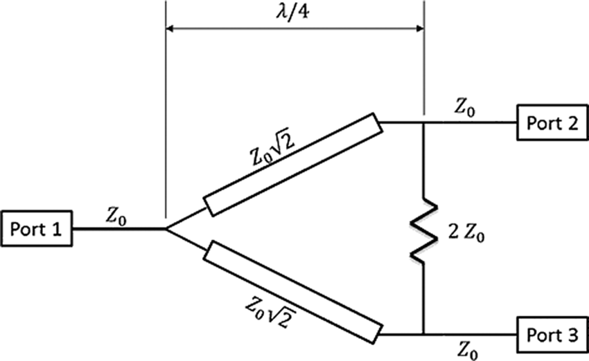
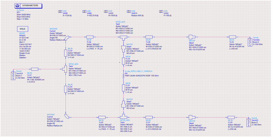
I kicked things off in ADS by building the schematic. The Wilkinson divider’s classic topology—quarter-wave transformers and a 100-ohm isolation resistor—formed the backbone. Using ADS’s built-in microstrip models, I accounted for the RO4003C substrate properties and discontinuities. After some tweaking, I ran the S-parameter simulation across 5650–5925 MHz.
Here’s the schematic I designed:
And the results? They hit the mark beautifully:
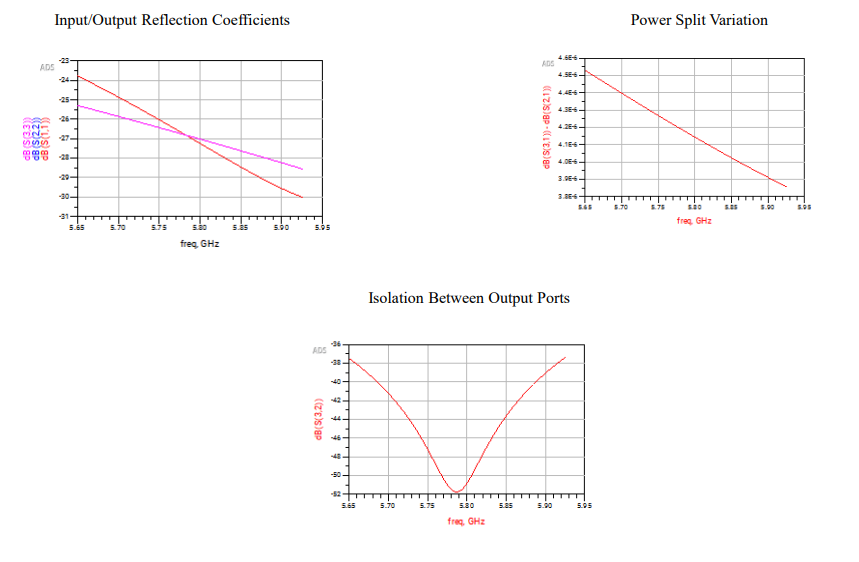
- S11: Well below -20 dB, showing excellent input matching.
- S22 and S33: Both under -20 dB, confirming solid output matching.
- Power split (S21 vs. S31): Within ±0.2 dB, nailing the equal split requirement.
- Isolation (S32): Better than -35 dB, meeting expectations.
I was stoked to see all specs met at the schematic level—full points in the bag there!
Step 2: Layout and EM Co-Simulation
Next, I translated the schematic into a layout view, ensuring every piece fit together without gaps or overlaps. This step was tricky—microstrip lines had to be precisely dimensioned, and the T-junctions and bends needed careful attention to avoid parasitic effects. Once satisfied, I fired up Momentum Microwave for the EM co-simulation.
Here’s the layout:

And the EM results:
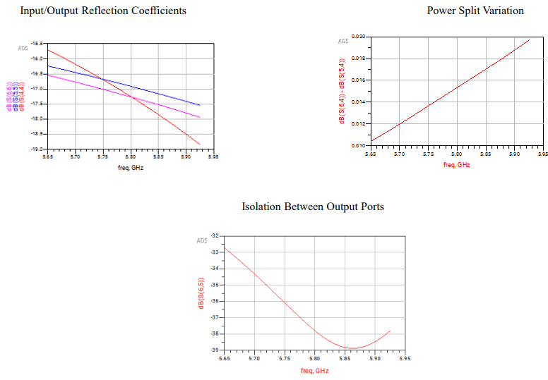
The EM simulation introduced some real-world deviations—parasitics and substrate effects slightly shifted the performance. While the project didn’t require the EM results to meet the Table 1 specs (phew!), it was a great reality check on how physical implementation impacts design.
Reflections
This project was a fantastic blend of theory and practice. Debugging the schematic to hit those tight specs taught me patience, while the layout and EM simulation drove home the importance of physical design. Collaborating with classmates on Ed Discussion was a lifesaver—bouncing ideas around helped me refine my approach.
If you’re an RF enthusiast or tackling a similar project, I’d love to hear your thoughts! For now, I’m proud of my Wilkinson divider and ready to take on the next challenge.
